A soft 16-Bit micro processor
Project Description
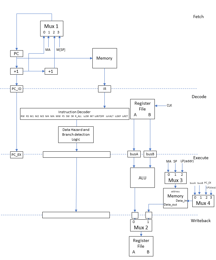
The goal of this project is to design a 16-bit microprocessor that can be used to generate a bit stream to program a Zybo Z7-10 FPGA The microprocessor has a 16-bit data bus and 12-bit address bus that enable accessing of up to 4096 16-bit memory locations. The memory block functions as a program memory, data memory and a top empty stack addressed from the last memory loaction (4095). The microprocessor uses a load-store architecture, in which data can be written to any memory address using only a specific set of instructions. It also has a basic single level interrupt facility that enables program flow change upon the occurrence of an external hardware interrupt. When this interrupt is triggered, the program enters an interrupt service routine. The instructions for a program are stored from address 0 in the memory and instructions for interrupt service routines are stored from address 512 (INTVEC).
Tools used
- Verilog
- Xilinx Zybo Z7-10 FPGA
Block Diagram

Test Programs and Results
Load two numbers from memory and run some basic math operations on them
			CLA //Clear A
			CLB // Clear B
			LDB M[260] //Load to register B from address 260
			LDA M[258]
			CMB //Complement B
			INCB //Increment B
			ADD //Add contents of register A and B
			LDB M[259]
			AND //And contents of register A and B
			STA M[1280] //Store contents of A to address 1280
			LDB M[1280]

This program reads an array of numbers from memory and pushes each to the stack them pops each number and adds to a running total using the JMP instruction. The result is then stored into memory.
    LDA M[82]
    PUSH A
    LDA M[83]
    PUSH A
    LDA M[84]
    PUSH A
    LDA M[85]
    PUSH A
    LDA M[86]
    PUSH A
    LDA M[87]
    PUSH A
    CLA
    LDB M[80]
    STB M[80] //keep track of counter
    LDB M[90] //get current sum result
    POP A
    ADD
    STA M[90]
    LDB M[80] //load counter value
    CLA
    DECB
    ADD
    SZ
    JMP 14
